The duotec glossary is your reliable source for quickly and accurately understanding terms like Chip on Board, thick-film technology, software development, electronics protection, and automation cell. It helps customers and partners gain deeper insights into our innovative solutions and technologies, enabling them to unlock their full potential. And if any questions remain unanswered, we are always here to provide personalized support—together, we make even complex topics easy to understand!
No fear of tight spaces – the art of microsystems integration.
Massive reductions in the size of semiconductors while simultaneously improving the performance of integrated circuits – the trend toward miniaturization continues. Assembly and interconnection technology (AVT) connects microelectronic components with other elements, such as PCBs, to create an electronic system assembly. Hybrid microsystems and microcomponents – such as printed circuits, electronics, and sensors in the smallest of spaces – offer significant innovation potential for novel and intelligent products across various industries and applications.
The growing diversity of applications in sensor and microsystem technology constantly presents new challenges for AVT and the packaging of miniaturized assemblies. Consistently high-quality and cost-efficient alignment and assembly of microcomponents can only be achieved through appropriate automation.
To manufacture highly integrated and miniaturized assemblies tailored to customer needs, we employ the following processes:
The most suitable AVT, efficient material management, and appropriate testing methods – our process development ensures the production of competitive and reliable products. The focus is on optimizing production times and costs while meeting the highest quality standards. Additionally, we aim to tailor processes precisely to customer requirements and needs.
Automation
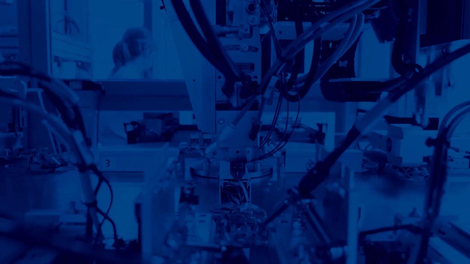
Equally important is the transition of products into series production. We achieve this using state-of-the-art technologies such as robotics, smart camera systems, sensors, and much more. Additionally, we develop automation solutions for high-volume production and manage change orders throughout the project lifecycle. For even more complex requirements, we collaborate closely with an external system integrator who brings over 10 years of experience in process development. This includes machine design, software development for system control, and robot programming.
Create a short, effective, and optimized process.
When developing and manufacturing specialized electronics, two questions regularly arise: What does it cost, and how long will it take? The answer is always the same: As little as possible. Even in the early stages of electronics development, we keep a close eye on costs. In process development, we optimize all manufacturing workflows to minimize time and costs while continuously improving quality. With the best possible solutions for assembly and interconnection technology and the most suitable selection of components, we guarantee a short, effective, and optimized electronics manufacturing process. And with the right testing strategy, we achieve maximum fault coverage without losing sight of the effort required for testing tools and times.
Process Development and Automation
3D layouts for optimal interaction between electronics and mechanics
Highly miniaturized implementation of assembly and interconnection technology
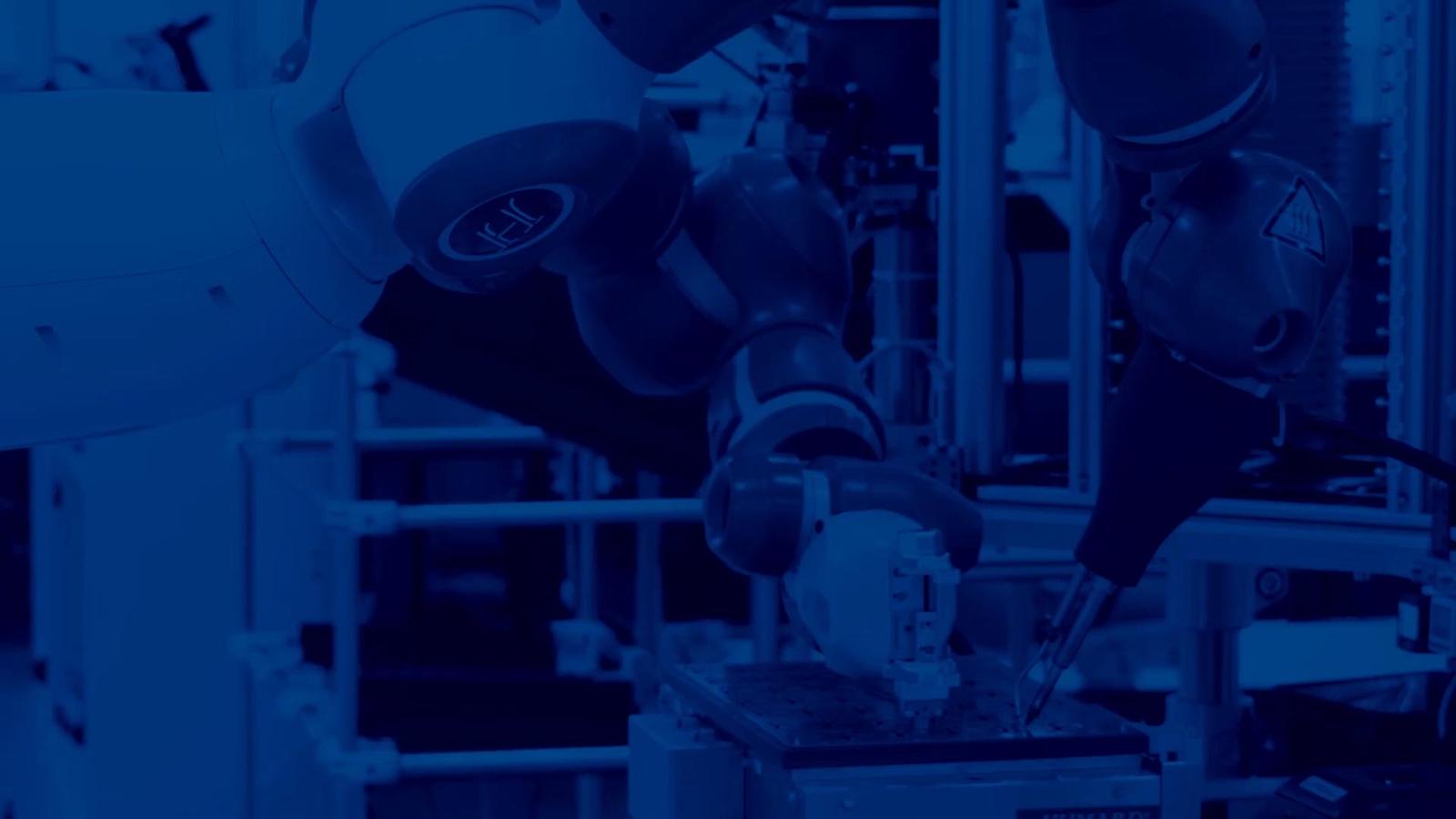
In the manufacturing of electronic assemblies and modules, an automated production cell lends us a helping hand. The perfect keyword here, as the single robotic arm features six axes and forms the centerpiece of a rotary indexing table. With the automation cell, we can carry out handling processes as quickly and efficiently as possible — from testing and assembling to gluing, welding, packaging, and labeling.
However, there’s no need to commit, as the twelve available stations are modular — meaning the equipment and joining tasks are interchangeable. Only the master module and the module mounting plates are part of the machine's base. When it comes to speed and flexibility, we’re setting new standards with the production cell — 12 times faster than usual.
Box-build involves the integration of electronics and mechanics into an optimized device solution and includes all assembly work on an electromechanical unit – except for PCB assembly. Box-build solutions by duotec are always tailored to customer specifications.
Our advanced assembly capabilities, in-house tool manufacturing, and complete logistics management reduce interfaces (one-stop shop), minimize time and logistics efforts, and enable faster time-to-market. Our customers receive a complete solution, including the housing, required cables, and – if desired – custom packaging.
For system integration, various housing materials are possible, and monitored screw technology ensures maximum precision during assembly. Additionally, we offer all necessary testing procedures and can also handle the programming and configuration of complete devices upon request, including the connection of pre-assembled cables.
Box Build at a glance.
Assembly of devices and switchgear, including module, functional, and system testing
Housing design
System and PCBA 3D modeling
Packaging, e.g., overmolding and potting technology
The CoB (Chip-on-Board) technology is an assembly process with relatively low production costs, yet it offers high miniaturization potential and considerable complexity in its structure. It ensures excellent thermal connection to the substrate material. We assemble bare semiconductor chips, known as "dies," in cleanrooms of classes 5 and 7 on ceramic or conventional FR printed circuit boards.
Subsequently, we connect them using wire bonding or solder/plastic on the circuit board. The bonding wires, made of gold or aluminum, are extremely delicate, with a diameter of only about one-third of a human hair. The bonded chips are coated with a glob-top made of plastic, providing secure protection.
Chip-on-Board offers great design flexibility and efficient thermal management.
Chip-on-Board
High miniaturization potential for electronic assemblies
Onto the substrate at a thickness of 200 micrometers.
The thick-film hybrid technology is an assembly and interconnection technology used to manufacture electronic components and integrated circuits in microelectronics. At duotec electronics manufacturing, we use thick-film technology to produce multilayer circuit boards and hybrid circuits. Electronic structures or conductor paths are directly printed onto ceramic, aluminum, or glass substrates using the screen printing process. The applied structures are tiny – only 200 micrometers wide, which corresponds to just 0.2 millimeters.
With thick-film hybrid manufacturing, we can even create crossing conductor paths by using insulating layers. The application of the various layers is achieved through repeated printing, drying, and sintering of each of the thick film paste layers in an 850-degree Celsius conveyor oven. Resistors, which are also printed, are then trimmed to the desired value using a laser.
After completing all printing processes, we compare the produced circuit with the target product and assemble additional components using SMD or THT placement, followed by soldering. More complex circuits can be applied to the substrate using integrated semiconductors via CoB (Chip-on-Board) technology.
Thick-film hybrid technology supports the miniaturization of electronic assemblies, ensures good thermal conductivity, and enables their use under extreme conditions.
Thick-film hybrid technology
More than 30 years of thick-film expertise (development and production since 1988)
Thick-film hybrid technology in the LabFab, including development and testing of thick-film-paste types
Preparation for series production
Use of ceramic substrates (Al2O3, AlN), aluminum, and glass substrates
Conductor track printing as well as resistor printing and laser trimming
We stand for Design for Excellence (DfX), which means striving to adapt the product's design to manufacturing, assembly, and testing processes while achieving the best possible cost structure. "Manufacturing begins with development at duotec" is therefore meant quite literally: Our product development, in close coordination with project management, adapts the electronic concept to series production in such a way that cost-effective manufacturing with high-quality standards is achieved.
Duotec takes the concept of Design for Manufacturing (DfM) even further: it’s not just about high-quality and cost-optimized electronics, but also about exceptional reliability and outstanding durability. To achieve this, we leverage our extensive application expertise and many years of experience in developing electronic solutions for various, and sometimes even extreme, application areas.
Direct overmolding is a special electronics protection process within our manufacturing techniques. After the electronics are assembled, the circuit board is placed into a mold and directly overmolded with a polymer — hotmelt, thermoplastic, or thermoset — using an injection molding machine. With clever material pairing, even cable sheaths or wire strands can be fused directly with the housing during this step. The advantage: assembly and encapsulation take place within seconds, as a homogeneous plastic housing forms a protective monoblock around the electronics.
Direct overmolding
Electronics protection process with short cycle time
High reproducibility of manufactured products
No additional external housing required
Sealed housing with IP68 protection class, 100% media-tight
Minimum wall thicknesses of 0.4 millimeters possible, meaning low space requirements and lightweight design
High robustness, integration of cable strain reliefs possible
Integration of connectors and light guides without separate assembly possible
LED integration possible
Good thermal conductivity
Minimal signal attenuation when overmolding sensors
High miniaturization potential
Production of large batch sizes
We also develop application-specific injection molds for your electronics.
Specific application area: medical technology
In medical technology, there is an increasing presence of motorized or battery-powered devices. These are used in minimally invasive or robot-assisted surgery as well as in endoscopy. Many devices need to be reusable and capable of being sterilized for their next use. Specifically, this means that the electronics and sensors used must withstand the special conditions of autoclaving – temperatures up to 140°C, a humid environment, and a washing cycle with chemical cleaning agents. Additionally, there are high demands for safety and reliability. The protection must also be economically competitive.
Autoclavable direct overmolding
The use of chemically and thermally resistant plastics in direct overmolding makes the protected assemblies washable and sterilizable. The overmolding exhibits high thermal stability at autoclaving temperatures between 134°C and 137°C. It also has excellent hydrolysis resistance and good chemical resistance to common, mostly alkaline cleaning agents. Up to 2,500 autoclaving cycles are possible. Furthermore, the use of biocompatible plastics is also an option.
Sleek design with plenty of functionality — printed electronics on glass
The printing of electronics on glass is a technology we have been offering since 2014 and have continuously developed ever since. Complex circuits can be applied directly onto glass using thick-film hybrid technology. Electronics printing on glass is not only highly functional but also meets the highest aesthetic standards.
Electronics printed on glass offer numerous applications in lighting, building technology, and medical technology. They can be used as touch panel control units or for basic applications such as LED lights. They are also a welcome addition to the furniture industry — for example, as LED lights embedded in glass display cabinets. Electronics for light sources can be printed directly onto a glass pane, transforming furniture pieces into interior design accessories with a contemporary design language.
Advantages of printed electronics on glass:
For touch panels, no additional circuit board for sensors is required
Multilayer conductor levels for higher circuit density and the implementation of additional shielding surfaces
Possible integration of lighting as well as control and display elements on glass components
Color printing with ceramic inks for excellent adhesion to glass, high color density, and exceptional durability and UV resistance
The protection of electronics generally pursues several objectives: Electronic components should be effectively safeguarded against external influences such as vibrations, moisture, dust, or chemicals for as long as possible. The goal is to ensure a long service life while avoiding costly maintenance and repairs. In short, the aim is to save unnecessary costs. Additionally, electronics protection ideally fulfills other functional or even aesthetic properties.
In certain applications, electronics protection must also work in the opposite direction, ensuring that no hazardous substances from the electronics escape into the environment or the medium being measured. For a sensor, it must also be ensured that the electronics protection does not impair signal quality. As part of our electronics manufacturing, we offer various protection methods.
Direct overmolding with polymers (also available as autoclaveable overmolding)
Enclosure assembly/box build
In every case, we tailor the electronics protection method and materials specifically to your electronics. Functional and fastening elements are protected as well. Our services also include 3D shaping and the production of housing components. Finally, tests are conducted to ensure electrical functionality and the effectiveness of the protection.
Good electronics protection offers many advantages
Improved thermal conductivity
Extended temperature operating range
Enhanced electrical insulation
Better heat distribution
Resistance to UV radiation, abrasion, and color changes
Ability to sterilize overmolded assemblies through direct overmolding.
In system integration, various housing materials are possible, and monitored screw technology ensures maximum precision during assembly. Additionally, we have all the necessary testing procedures and can also handle the programming and configuration of complete devices upon request, including the connection of pre-assembled cables.
Box Build at a Glance.
Assembly of devices and switchgear, including module, functional, and system testing
Housing design
System and PCBA 3D modeling
Packaging, e.g., overmolding and potting technology
We offer a special service within our manufacturing services at our Greifswald site: Here, we not only produce electronic components but also take over entire production lines — for example, for the last three to five years of production. This includes taking over product manufacturing according to customer specifications.
ml&s in Greifswald not only has the necessary space but also the required technical expertise to continue operating older machinery efficiently. After the end of production (EoL), the customer decides whether to store or scrap the machines.
Fact: An electronic assembly only works with the right hardware — circuitry, components, and mechanics. The duotec service includes the review of these parts. We evaluate your idea, create a feasibility study, and draft the corresponding specification sheet. Then, the real work begins: For the functionality test of the electronics, we first develop a prototype.
This, along with an electronic and thermal simulation program, allows us not only to thoroughly test the electronics but also to verify whether the manufacturing process functions optimally. Finally, we design the mechanics in which the electronics will be embedded. Thanks to detailed 3D studies, we can simulate the perfect fit in advance.
Hardware development
Sensor systems for a wide range of measurement variables
Controllers and inverters in the field of power electronics
Control and regulation technology
LED technology for lighting concepts
Embedded Systems
Bus systems such as DALI, DMX, Interbus
Wireless systems such as Bluetooth Low Energy, JenNet-IP, Zigbee
Special tests from prototypes to the finished product.
As the complexity of assemblies increases, so do the requirements for testing procedures. To ensure quality, we therefore use optical, mechanical, and electrical tests—depending on the type of electronics.
The optical inspections
AOI test: Automatic Optical Inspection
AXI test: Automatic X-Ray Inspection
Electronic functional tests (universal or customer-specific)
Flying Probe
Functional Test (FCT)
Boundary-Scan Test - Standard method for testing digital and analog components
In-Circuit Test - Test of the electronic circuit (ICT)
Safety tests - High voltage (HV) special test system
Pre-programming of components with specific adaptations
Marking of components with software version as laser marking or with a label
The development and production of customer-specific electronics include a specific testing procedure. For electrical tests, we develop and build specialized testing equipment and program the appropriate test software.
Centralized data management plays a key role in this process: data exchange, maintenance, backup, and analysis are digitally secured and available on demand.
Inspection & Testing
In-house adapter and test equipment construction
Specialized test benches for devices and systems
Centralized data management
Adoption and support of customer measurement technology
Optimal functioning assemblies are based on optimally designed circuitry — function is only as good as its form. The challenge here is that the demands on PCB design have skyrocketed in recent years. Electronic components are becoming increasingly complex and smaller, while having to integrate a much greater variety of components in return. We develop PCB layouts that fully meet these requirements.
What's more, through PCB layout routing, we are also able to adapt existing circuit designs to meet your new requirements.
State-of-the-art — our PCB technology
With Altium Designer, we develop groundbreaking PCB designs or adapt circuits to the prevailing status quo. Our technologies are always state-of-the-art worldwide – whether it's new development or optimization.
Altium Designer
Multilayer PCBs
Rigid-Flex PCBs, Flex PCBs
IMS PCBs (Insulated Metal Substrates)
HDI PCBs (High Density Interconnects)
Thick Copper PCBs
Longboard PCBs
Ceramic Substrates
Glass Substrates
Ball-Grid-Array (BGA), Chip-on-Board (CoB)
Embedded Components
During the manufacturing of the PCB or circuit layout, we also take care of other relevant factors: the appropriate dimensions of the board, its highest possible miniaturization, high packing density, thermal management, and ensuring EMC compliance. At the same time, we design the assembly in 3D, allowing it to be fitted into a housing already during the layout phase. The special feature: Collision checks are performed during the layout development itself.
A populated circuit board only becomes a groundbreaking product with the right housing — a beautiful shell, a smart core. But there’s more: an enclosure protects the inner workings from a variety of harmful environmental influences. We determine which properties, especially mechanical ones, the housing needs as early as during the PCB layout development. Through realistic simulations, we identify the requirements the overall design must meet and the protection levels needed to achieve them. Ensuring EMC compliance is also integrated into this process. Early collision checks save a lot of time and money during later implementation.
Depending on the application area of the electronics and the associated challenges regarding protection class and standards, the technology can also be protected within the housing itself — a beautiful shell, a smart and self-protecting core.
In prototype construction and series production, it is essential to meet each customer's requirements precisely. Said and done: This process at duotec is structured and streamlined in such a way that it ensures low costs, fast delivery times, and a seamless transition to series production. It is now up to the client to decide, based on the aforementioned criteria, whether the prototype production will be fully automated, semi-automated, or entirely manual. At the same time, this step also involves determining whether the design and construction of the prototypes will be handled in-house or entrusted to us.
In addition to our many years of expertise in prototype construction and series transition, we also possess the specialized knowledge to select the best possible materials and processes for the goal of "mass production." Without question, the wishes of our customers take top priority.
Categories in prototype construction — from A to D:
Functional prototype (A)
Prototype (B)
Pre-series prototype (C)
Pilot series prototype (D)
In addition to the stages listed, we offer additional tests and measurements. If desired or even necessary, we compile the results and findings into a clear and concise report.
The New Product Introduction (NPI) or product launch is one of the most sensitive processes that our customers go through with us. From the initial idea to a market-ready product, i.e., within industrialization, a wide variety of steps are required. Ever-shorter product and innovation cycles make it essential to execute these steps faster and more efficiently.
This places high demands on an EMS and E2MS service provider, regardless of whether it involves high-mix-low-volume or low-mix-high-volume projects. With our cross-functional customer teams, consisting of procurement, product development, and project management, we bring your products to life with a short time-to-market and ensure rapid innovation cycles.
New Product Introduction
Optimal adaptation of circuit design, PCB substrate material, and electronic components
Reduction of component count through functional integration
For electrical testing, we develop and build specialized test equipment and program the appropriate test software at the same time. This allows us to directly address the requirements of your application.
Test equipment development
Special test benches for devices and systems
Custom-specific test adapters and fixtures
Universal test benches for small devices
Various functional test stations on self-developed test platforms (e.g., UTS system, Reinhardt, Spwa, and test bench (LabVIEW))
Adoption and support of customer measurement technology
System configuration, programming, parameterization
Electrical testing
EMC testing, environmental testing, high-voltage, burn-in, and climate tests
The foundation for the flawless functionality of an electronic assembly lies in a sophisticated layout, meticulously designed down to the nanometer. This also includes circuit design. Although the demands in this discipline are becoming increasingly complex and challenging, we are capable of combining even the most intricate requirements into a simple and clever circuit design.
circuit design
Designs for microcontroller circuits, embedded systems
AC/DC converters, DC/DC converters
Sensor frontends for signal conditioning of sensor elements
The best software is designed to complement the hardware.
For optimal functionality, there is only one solution: Embedded Systems Engineering — or metaphorically speaking: hardware and software are fraternal twins working hand in hand. With this holistic approach, we ensure from the very beginning that everything runs smoothly at the time of production. This level of precision requires a thorough requirements analysis and precise prototyping — and that’s exactly what we do!
Our software development services cover a wide range of areas. We utilize various microcontrollers — from low power to high performance, from low cost to high-tech. At the same time, we also rely on wired or wireless bus systems, interfaces, and communication protocols.
The list is long — see for yourself:
Wireless communication and networks for IoT, such as BLE / Bluetooth Smart, Zigbee
Custom-tailored automation technology: sensors, control, and regulation technology, e.g., for motors, valves, pumps
Device operation via touch or gestures
Experience in compliant implementation for safety-critical projects (medical technology, functional safety) with risk control measures and diagnostics
Additionally, we possess further expertise in the software universe — for example, we develop firmware and program microcontrollers.
Firmware for embedded systems of various types and complexities
From low-level drivers to abstract applications
From real-time operating systems (RTOS) to Embedded Linux
From object-oriented software development to assembly code
Bootloaders for software updates after delivery
Data processing, filtering functions, and signal analysis, DSP
Development and implementation of customer-specific algorithms, functions, and processes
And we don’t leave computers out of the equation in software development either.
Flawless operation of the assembly line, leaving nothing to be desired.
SMT assembly for all batch sizes.
SMT assembly enables not only high component density but also the miniaturization of circuits and assemblies. fabsolutions' SMD manufacturing services are carried out using high-speed placement machines for processing PCBs with components as small as size 01005. Unlike THT, surface mounting does not involve wire leads. Instead, components are directly fixed onto the PCB using the reflow process or wave soldering. Subsequently, the assembled PCBs (PCBAs) undergo AOI and/or AXI testing.
SMT at a glance.
High component density enables the miniaturization of circuits and assemblies
Double-sided PCB assembly possible
Improved electrical properties of the circuit, especially at higher frequencies
Faster production through pick-and-place
Increased manufacturing quality through automated PCB assembly
No contamination
Reduced lead times through the use of Manufacturing Execution System (MES) software
The SMT production is designed as an in-line concept and allows for a high degree of automation — even for high-volume production of the smallest components. It includes laser marking of PCBs, solder paste printing, placement, reflow or selective soldering with multi-wave, flux removal, AOI and ICT, as well as a depaneling robot that separates the panels and prepares them for packaging. All PCBs are fully traceable. Defective PCBs are identified via AOI and are not further processed.
The development and production of a customer-specific electronic assembly also includes tailored test development. The more complex the device, the more demanding the manufacturing process and testing procedure become.
Test development covers a wide range of testing processes — such as system configuration, programming, or parameterization. And for everything, we have a test.
Test development
In-Circuit Test - Testing of the electronic circuit (ICT)
Functional Test - Functionality test (FCT)
Run-In Test - Assembly reliability test
Burn-In Test - Simulation of assembly aging
Boundary-Scan Test - Standard method for testing digital and analog components
Our manufacturing technologies also include THT assembly. Components subjected to high mechanical stress, such as connectors, switches, or power semiconductors, are rarely available in SMD designs.
We primarily assemble wired components manually — supported by automated processes of the pick-to-light system. Axially and radially wired components can be assembled automatically without limitations. With fully automated soldering processes (Through-Hole Reflow Technology), wired components can be soldered in a reflow oven, eliminating the need for costly manual or wave soldering.
All mixed-assembly circuit boards are inspected using AOI.
Beyond our own electronics manufacturing, we also have a fully functional toolmaking department. This means: we are not only capable of producing the solution but also manufacturing the means to achieve it. The key advantage here is that we can significantly reduce the time between development and production. Additionally, our in-house toolmaking offers several other benefits:
Fast maintenance and repair
A single point of contact for the customer (one-stop shop)
Production of in-house prototype tools and fixtures